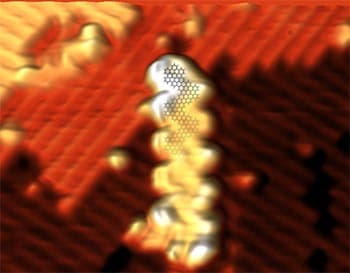
Atomically precise chevron-shaped graphene nanoribbons were purified after solution synthesis, cleanly placed by dry contact transfer on a hydrogen-passivated Si surface, imaged and manipulated by scanning tunneling microscopy, and covalently bonded to depassivated surface positions.
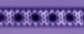
The ability to dope graphene nanoribbons with boron atoms to atomic precision opens a range of possible new applications, from chemical sensing to nanoelectronics to photocatalysis to battery electrodes.
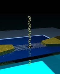
A nanoribbon transistor no thicker than the distance between adjacent DNA bases provides high resolution sensing of DNA passage through nanopores, perhaps leading eventually to rapid DNA sequencing.
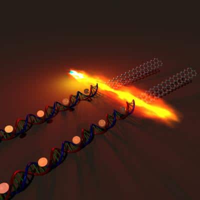
How complex could circuits be made using precisely positioned DNA nanostructures as templates to grow graphene nanoribbons?
Two research groups have published two different ways to unzip carbon nanotubes to create graphene ribbons.
BuffYoda writes "BERKELEY, CA — "Another important step towards realizing the promise of lightning fast photonic technology has been taken by scientists with the U.S. Department of Energy's Lawrence Berkeley National Laboratory (Berkeley Lab) and the University of California at Berkeley. Researchers have demonstrated that semiconductor nanoribbons, single crystals measuring tens of hundreds of microns in length, but only a few hundred or less nanometers in width and thickness (about one ten-millionth of an inch), can serve as 'waveguides' for channeling and directing the movement of light through circuitry." An interesting (though by no means unexpected or revolutionary) development in photonics, a field I consider to be of great importance to the development of extremely fast computers (this route seems to be a lot closer than the alternatives)."
Presenters Joe Lyding, Beckman Institute Joe Lyding is a distinguished professor in Electrical and Computer Engineering at the University of Illinios. His career includes constructing the first atomic resolution scanning tunneling microscope, discovering new industrial uses for deuterium, studying quantum size effects… Read More Leonhard Grill, University of Graz Leonhard Grill is a professor at… Continue reading J. Lyding & L. Grill | Silicon-Based Nanotechnology & Manipulating Single Molecules on Surfaces
Summary An overview of projects spearheaded by the Advanced Manufacturing Office of the US Department of Energy. These projects, involving Atomically Precise Manufacturing, are part of a larger vision for energy efficiency. The diverse portfolio of projects includes molecular assembler tips, molecular lego, diamondoid tools, copper/carbon hybrid materials, DNA origami, and Microelectromechanical systems. Presenters Tina… Continue reading AMO’s Program in Atomically Precise Manufacturing and Nanocarbon Metals | Tina Kaarsberg, DOE
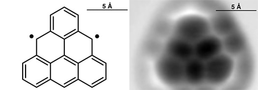
A molecule with two unpaired electrons too unstable to be made by chemical synthesis was fabricated using a scanning probe microscope to remove two hydrogen atoms from a single molecule adsorbed to a copper surface at ultra low temperature and ultra high vacuum.
A review article presents the amazing features of graphene and discusses how it might complement or replace silicon for the fabrication of electronic devices.